A 6 kV rectifier chosen for current, not for voltage
The HV37-06F is an axial-leaded fast recovery high voltage diode rated at 6 kV repetitive peak reverse voltage and 500 mA average forward current in air at 40 °C, with a 75 ns recovery time. It is the lowest-voltage and highest-current member of the HV37 range, which makes it the sensible starting point when your circuit peaks below 6 kV and the rectifier — rather than the blocking voltage — is what limits the design.
The body is a black moulded epoxy cylinder with the model and rating printed on it and a band at the cathode end. Its two straight leads solder into through-holes or terminal posts, so the part suits assemblies that are hand-built, rebuilt or encapsulated after soldering rather than run through a reflow line. Under the moulding the chip carries a passivation glue layer, so contamination and moisture have two barriers to cross before they reach the junction — the construction detail that lets a body this small hold 6 kV.
Typical work is rectification inside the high-voltage tank of medical imaging generators, NDT and X-ray inspection sets, DC high-voltage test gear, radar supplies and compact assemblies that are potted once wired. It also replaces older glass-passivated axial rectifiers in equipment being rebuilt rather than redesigned, where the footprint and lead spacing already exist and only the diode changes.
Every part is built to the same construction and test sequence as the rest of our high voltage diodes, so a design evaluation unit and a production batch behave the same way in your circuit.
- Axial leaded connection. Two straight leads solder into through-holes, terminal posts or a socketed fixture, so the part works in hand-built, rebuilt and potted assemblies without a reflow profile or a stencil. - High thermal conductivity epoxy moulding. The compound moves heat from the chip out to the body surface, which means cooling the body is what sets the limit rather than the moulding holding heat in. - 75 ns recovery time. Switching loss stays small in high-frequency rectification, and the diode does not become the element that sets the timing of a pulsed circuit. - Special passivation glue chip protection. A passivation layer sits on the chip before the epoxy goes on, so contamination and moisture face two barriers before they reach the junction. - Excellent discharge characteristics. Behaviour stays predictable in capacitor-discharge and pulse-forming circuits that hit the diode with repeated fast edges. - 15 A surge forward current. The datasheet allows 15 A for 0.01 s on a 50 Hz half-sine, which covers the inrush of a cold-start high-voltage supply. - The current-maximum member of the range. 500 mA in air at 40 °C is the highest average forward current among our high voltage diodes, and it comes at the lowest blocking voltage — useful when current, not voltage, is the real constraint. - Stable across a wide window. Operating and storage both run from −55 to +125 °C, so the part takes transport, storage and a cold start without a warm-up step.
| Package drawing | The mechanical sheet for the footprint, terminal post or potting shell check, so layout sign-off and electrical sign-off can run in parallel instead of one waiting on the other. Installation guide | Soldering, lead forming, cleaning, drying and encapsulation in the order we recommend, plus the operating media we suggest for this high voltage diode. Insulation adhesive reference | Cured state and strengths for silicone, acrylic, urethane and epoxy systems, so the potting decision is filed with the diode rather than made at the bench on the day of build. Incoming inspection points | Two reverse leakage references, 2.0 µA at 25 °C and 10.0 µA at 100 °C with VRM = VRRM, give your inspector values to compare against instead of a pass mark with no condition attached. Marking and lot code | The model, rating and cathode band printed on the body, and the code that ties a delivered part back to its build record. Declarations for your file | Tell us which declarations your quality department needs; as high voltage diode manufacturers we confirm in writing what we can support for this model rather than leave a gap in your approval file. |
| Parameter | Value |
|---|---|
| Part number | HV37-06F |
| Repetitive peak reverse voltage (Vrrm) | 6 kV at Ta = 25 °C, Ir = 2.0 µA |
| Average forward current, in air (If2(AV)) | 500 mA at Ta = 40 °C |
| Average forward current, in oil (If2(AV)) | 300 mA at Ta = 55 °C |
| Backward recovery time (Trr) | 75 ns |
| Surge forward current (Ifsm) | 15 A, 0.01 s half-sine, 50 Hz |
| Forward peak voltage (Vfm) | ≥12 V |
| Reverse leakage at 25 °C (Irrm1) | 2.0 µA at VRM = VRRM |
| Reverse leakage at 100 °C (Irrm2) | 10.0 µA at VRM = VRRM |
| Operating ambient temperature (Ta) | −55 to +125 °C |
| Storage temperature (Tstg) | −55 to +125 °C |
| Termination | Axial leads, cathode end banded |
Two current figures, two test conditions
The datasheet gives two average forward current values, and they are regularly read as a contradiction. They are not. The 500 mA figure is measured in air with the ambient held at 40 °C; the 300 mA figure is measured in oil with the ambient at 55 °C. The higher number is not a bonus for air cooling and the lower one is not a penalty for oil — they are two points on the same thermal curve, taken at different temperatures and in different media.
For your own design, take the figure measured closest to your real conditions and keep margin on top of it. An assembly sitting in still air at 55 °C is outside both test points, so it needs forced air, a heat-spreading surface, or a lower operating current agreed with our engineers before the design freezes.
Why the thermal ceiling matters as much as the current number
Both the operating and the storage range stop at +125 °C. With a forward peak voltage in the ≥12 V region, this high voltage diode dissipates real power at full current, and body temperature is ambient plus that rise — the limit applies to the part, not to the room. Blocking quality drifts with heat too: reverse leakage is specified at 2.0 µA at 25 °C and 10.0 µA at 100 °C, so a hot diode is a leakier diode. Thermal design protects the voltage margin as much as it protects the current rating.
Surge is not sustained overload
The 15 A rating is a 0.01 s half-sine at 50 Hz. That covers the inrush of a cold-start supply or a single fault event; it is not a licence to run the part above its average current, because repetitive pulsing heats the chip in a way the surge figure does not describe.
Choosing the voltage step
Inside this family, blocking voltage and current trade against each other: the 6 kV member carries the most current, and each step up in voltage gives some of it back. Move up a step only when your peak reverse voltage with margin genuinely needs it, then re-check the resulting current against your cooling.
- Where the failures come from. In service, high voltage diodes fail from four directions — voltage stress, heat, surface condition and handling — and each one can be checked before a design is signed off. - Repeated overvoltage above the 6 kV rating. A part that goes short or open after weeks of service has usually met a peak reverse waveform higher than the rating: look at the recovered edge with the assembly in its final potting, and if the peak keeps climbing past 6 kV, the 8 kV HV37-08F is the next step in the same family. - Heat judged by the room instead of the body. 500 mA holds with 40 °C air; the same current inside a 70 °C enclosure puts the body above the 125 °C ceiling, because with a forward peak voltage of ≥12 V the diode dissipates real power and the limit applies to the part, not to the ambient. - Leakage that heats its own junction. Reverse leakage climbs from 2.0 µA at 25 °C to 10.0 µA at 100 °C, so a warm assembly leaks more, dissipates more and runs hotter — a loop that ends in thermal runaway or a supply tripping on overcurrent. - Surge read as continuous current. The 15 A figure is a 0.01 s half-sine at 50 Hz, covering a cold-start inrush or a single fault event; it describes nothing about repetitive pulsing, which is already governed by the average forward current rating. - Contamination on the surface, not inside the part. Flux residue, fingerprints and condensation build the leakage path across the board between the leads long before anything crosses the epoxy. - Stress at the lead-to-body seal. A long soldering dwell, an iron resting near the body or a bend formed tight against the epoxy damages the joint, and the damage surfaces later as leakage or an open circuit. - A potting compound working against the part. A rigid adhesive over a body that cycles through wide temperature swings can crack away from the epoxy or leave a void that becomes a discharge site; match the compound to the medium and to the swing the assembly actually sees.
| Adhesive | Cured state and characteristics |
| Silicone — cured state | Transparent, elastic rubber after curing |
| Silicone — strengths | High shock absorption; absorbs the stress of large temperature swings from −40 to 200 °C |
| Acrylic — cured state | Transparent, hard coating |
| Acrylic — strengths | Low moisture absorption, fast cure, excellent wear resistance and insulation |
| Urethane — cured state | Transparent, hard coating |
| Urethane — strengths | Excellent wear resistance and good moisture resistance; stable at low temperature but less tolerant of high temperature |
| Epoxy-based — cured state | Very sturdy and usually opaque |
| Epoxy-based — strengths | Good moisture, chemical and wear resistance, with good dielectric properties |
Selection starts with your circuit, not a catalogue number: tell us the working voltage, load current, switching frequency and ambient cooling conditions, and our engineers will match a model from our range and explain the margin left in the design. Each model ships with its datasheet, package drawing and installation guide, and we stay available for mounting and soldering questions, start-up checks and fault finding when an existing part runs hot or fails early. Orders run from about 7 days to 6 months depending on quantity, usually by international express.

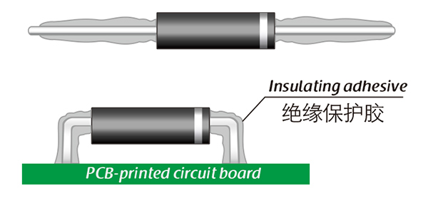
Here, suitable insulation adhesive materials can be selected based on the different usage situations of engineers.